SRAM design
At Arm, I work on SRAM circuit design and characterization at advanced technology nodes. My work includes circuit sizing, timing and power analysis, and checking read and write margins across process, voltage, and temperature conditions.
I work on SRAM circuit design and characterization at Arm in Noida. My research background spans arithmetic circuits, AI accelerator architectures, and memory systems.
My Ph.D. at IIT Gandhinagar, under Prof. Joycee Mekie, focused on energy-efficient hardware for AI—improving how hardware computes and how it stores and moves data through approximate computing, posit arithmetic, and in-memory computing.
Alongside my engineering work, I write about semiconductors and share learning resources for students interested in VLSI.
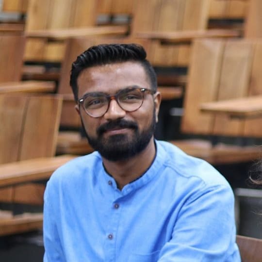
At Arm, I work on SRAM circuit design and characterization at advanced technology nodes. My work includes circuit sizing, timing and power analysis, and checking read and write margins across process, voltage, and temperature conditions.
My doctoral research addressed both compute and memory costs in AI hardware. I worked on approximate arithmetic, posit-based DNN accelerators, and analog and digital in-memory computing, connecting circuit choices with application-level energy, performance, and accuracy.
I have taught IC design, supported NPTEL courses, and mentored students on VLSI projects. I also write about memory design and semiconductors on LinkedIn, using circuit examples to explain the ideas.
My doctoral research approached AI hardware as a system: the cost of arithmetic, the size of the data representation, and the energy spent storing and moving that data all matter. I explored two connected ways to improve it.
I explored approximate adders, multipliers, and dividers, alongside posit number representations for DNN accelerators. The aim was to reduce energy, area, and execution time while meeting application accuracy requirements. Choosing the number format and precision also changes the storage footprint and data-transfer cost.
Arithmetic & accelerator researchI developed analog and digital in-memory computing circuits and studied memory architectures to address the cost of moving data between storage and compute units. This work included SRAM compute circuits, sense amplifiers, process-variation resilience, and tools to evaluate architectural trade-offs.
Memory & in-memory computing researchHardware–software codesign connects these choices: an efficient arithmetic unit must work with the accelerator’s dataflow, buffers, and memory system to improve the complete design.
A capacitive multiplier for analog in-memory computing in 6T SRAM, designed to reduce the effect of process variation on multiplication.
A current-domain approach to analog in-memory computing that addresses the effect of process variation on computation accuracy.
Approximate posit arithmetic and DNN accelerator codesign, connecting compute efficiency with lower storage and data-transfer requirements while evaluating neural-network accuracy.
I spoke with students about VLSI career paths and how circuit design, timing, and engineering decisions connect academic learning with industry work.
Event detailsA talk about my path from doctoral circuit research at IIT Gandhinagar to memory design at Arm.
Event programmeA conversation about starting a Ph.D. after B.Tech., research at IIT Gandhinagar, the PMRF fellowship, and VLSI career paths.
Watch on YouTubeHow does a memory cell store data? Why is writing harder than reading? What sets SRAM Vmin? I explore these questions through circuit examples.
Read the seriesI grew up in Arunachal Pradesh and studied Electronics and Communication Engineering at NIT Arunachal Pradesh before joining IIT Gandhinagar through the Start Early Ph.D. programme.
At IIT Gandhinagar, I worked with Prof. Joycee Mekie in the nanoDC Lab on energy-efficient AI hardware. My thesis, Domain-specific hardware design with emphasis on energy efficiency, performance and robustness, brought together approximate computing, posit arithmetic, and in-memory computing. I also taught IC design.
I submitted my thesis in May 2023, joined Arm in Noida in October 2023, and defended my thesis in June 2024. I now work on SRAM design and characterization, while continuing to write about semiconductors and mentor students.
View my CVSenior Design Engineer, Physical IP Group.
SRAM circuit design and characterization at advanced technology nodes.
Electrical Engineering, nanoDC Lab.
Start Early Ph.D. programme.
Advisor: Prof. Joycee Mekie.
Research: energy-efficient AI hardware across compute and memory.
Thesis submitted: May 2023
Thesis defended: June 2024
Electronics and Communication Engineering.
Chairman Gold Medal and Institute Gold Medal.
At IIT Gandhinagar, I taught the Digital IC Design Lab as a Graduate Teaching Fellow and supported other courses as a teaching assistant. I also worked as a tutor for NPTEL’s Digital Circuits and Design and Analysis of VLSI Subsystems courses.
I share presentations, programming tutorials, and recorded tutorial sessions. Each resource lists my contribution, collaborators, and course instructors.
All learning resourcesDuring my Ph.D., I received the Prime Minister’s Research Fellowship and Intel India Research Fellowship in 2020. I was also an SRC Research Scholar.
I received IIT Gandhinagar’s Outstanding Graduate Teaching Fellow Award in 2022 for my work teaching the IC Design course.
I served as Track Co-Chair for ULSI Circuits, System-on-Chip, and Power SoC at ICEE 2025. I also review research papers and collaborate with students and researchers.
CollaboratorsLet's connect
For research discussions, invited talks, or conversations about memory design and VLSI education.